Designs and fabricates the transistors inside every computer, phone and weapon, using machines precise enough that only a few factories on Earth can run them.
Also called: Chip Engineer · IC Design Engineer · Process Engineer
Semiconductor Engineer: Designs and fabricates the transistors inside every computer, phone and weapon, using machines precise enough that only a few factories on Earth can run them.
A semiconductor engineer designs, builds or manufactures the integrated circuits that run almost every powered object on Earth, from a car's brakes to a nuclear-armed missile's guidance system. The work splits broadly into two camps: design engineers who lay out circuits in software and hand off a finished blueprint, and process or device engineers who run the physical factories, called fabs, that etch those blueprints into silicon a few atoms at a time.
The profession is younger than most on this site — the first working transistor was demonstrated in 1947 — but it has become one of the most consequential. A handful of companies, concentrated in a handful of places, now control the machines and know-how needed to make the most advanced chips, and every government with a stake in artificial intelligence, defense or economic growth has decided that matters enormously.
That concentration is what makes this job unusually high-stakes. A single Dutch company builds the lithography machines advanced chipmaking depends on; a single Taiwanese company fabricates the large majority of the world's most advanced logic chips; and export-control rules written in Washington now shape which countries an engineer can legally sell equipment or expertise to. Few engineering careers sit this close to great-power politics.
Inside the profession
A semiconductor engineer designs or fabricates the transistors inside nearly every powered device, working at tolerances so tight that a handful of factories and toolmakers constrain what the rest of the world can build.
Design, process and the wafer's verdict
The profession splits between chip design—architecture, RTL, physical layout, verification—and process or manufacturing engineering inside the fab. Designers learn that first silicon lies until it is measured; process engineers live by statistical process control, defect maps and split lots that change one variable at a time. Walking the fab before trusting a dashboard catches tool drift screens miss. Mask errors are unforgiving: a wrong pattern replicates across thousands of dies before anyone can soft-reset reality.
Cleanrooms, lots and yield
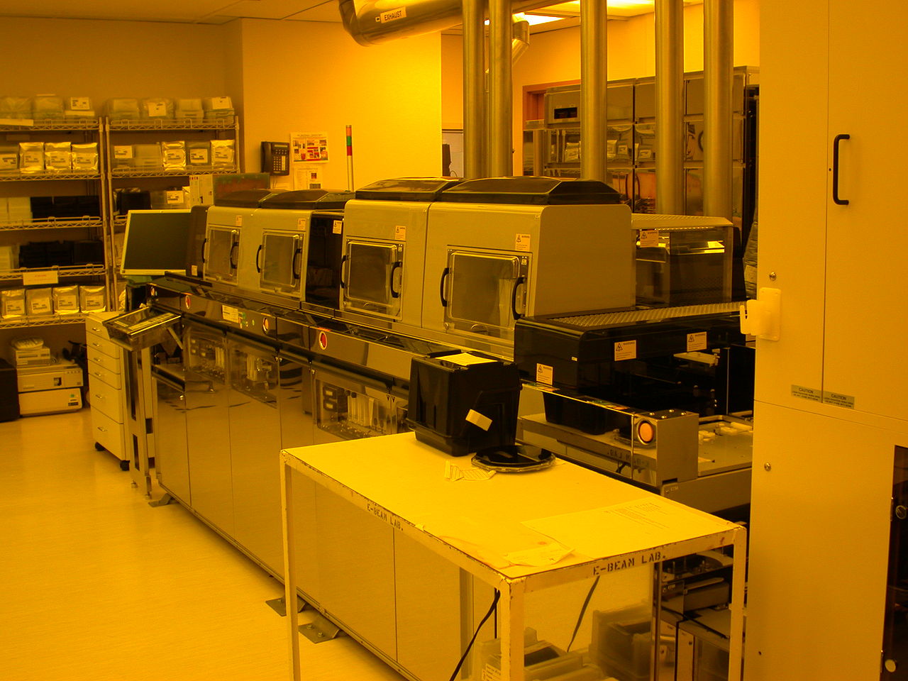
A manufacturing day starts with shift handoff: overnight lots, tool alarms and SPC charts from the outgoing crew. Gowning through airlocks, checking assigned tools and deciding whether to kill a lot before it poisons yield are practical judgments under cost pressure. Failure analysis with cross-sections and electrical test data turns a bad wafer map into a root cause. Equipment vendors' field engineers become daily collaborators. On-call weeks exist because a stuck tool does not wait for business hours.
Schools, screening and geopolitical gates
Strong pipelines run through NYCU and NCKU in Taiwan, KAIST in Korea, MIT, Eindhoven and other microelectronics centers, but the scarce resource is often fab access and mentor time on real nodes. Export-control screening and security clearances gate who may touch advanced process or defense-related design in the United States and allied systems. PE or CEng titles matter less than demonstrated tape-out or yield recovery stories. Concentration in Taiwan foundries, Dutch lithography and a few IDM campuses makes geography part of the career.
AI layouts and strategic geography
Machine-proposed layouts and exploding verification loads are shifting junior design work toward review and constraint crafting. AI accelerator design has become its own specialty atop classic CPU and mobile work. Geopolitics now relocates fabs and talent through industrial policy, changing where process engineers can practice leading-edge nodes. What remains human is deciding which experiment to run next, when to scrap material and whether a 'good enough' bring-up is actually shipping a latent field failure.
How the work branches
Five common shapes of the same title — specialty, setting or career path.
Fabless companies and IDMs
Digital design / RTL engineer
Implements architecture in hardware description languages and closes timing with verification teams before tape-out.
Design houses and foundry enablement
Physical design / PDK engineer
Places and routes transistors under process rules, fighting congestion, power and manufacturability constraints.
Fabs and foundries
Process / yield engineer
Owns tool health, SPC and experiments that recover yield when defectivity or parametric drift appears.
Advanced-node R&D
Device / integration engineer
Develops transistor structures and module integration where nanometer films and etch profiles decide performance.
Pre-silicon and bring-up teams
Verification / DFT engineer
Builds the testbenches and scan strategies that catch bugs before and after silicon, now often the schedule bottleneck.
How it reads by country
Same craft, different gatekeeping, status and daily texture — rewritten for readers in each language.
Fabless design and CHIPS Act fabs
US semiconductor careers skew toward fabless design, EDA, equipment and a rebuilding manufacturing base under industrial policy. Export controls, ITAR-adjacent screening and campus recruiting into Nvidia, Intel, AMD and suppliers shape early paths as much as pure academics.
Samsung, SK hynix intensity
South Korean engineers enter a memory-and-logic ecosystem dominated by Samsung and SK hynix, with KAIST and related schools as feeders. Shift culture in fabs, rapid node races and national strategic status make the job high-prestige and high-pressure.
Equipment, materials and revival bets
Japanese semiconductor work is strong in materials, equipment and specialized devices, with policy bets on regained logic capacity. Careful process discipline, supplier craftsmanship and long employment norms still colour engineering culture across firms.
Dresden, auto chips and Infineon
German engineers cluster around Infineon, automotive semiconductors and the Dresden fab corridor under EU Chips Act attention. Functional safety, industrial reliability and tight supplier links to carmakers define much of the daily craft beyond consumer phones.
Design houses and Arm's orbit
UK strength sits heavily in chip design, IP and research around Arm's ecosystem rather than leading-edge high-volume fabs. University spinouts, verification talent and specialized analog or AI design shops offer paths distinct from East Asian manufacturing intensity.
GlobalFoundries and regional hub roles
Singapore hosts major manufacturing and regional HQs, including GlobalFoundries' presence, inside a trusted logistics and talent hub. Process, packaging and operations engineering sit beside design support roles in a compact, export-oriented ecosystem.
From the archive
Commons CC/PD images self-hosted for this profession.
Why attitude matters here
A semiconductor engineer's tools can move atoms and close timing, but attitude decides whether a bad lot is killed early, whether one variable is changed per split, and whether 'good enough' silicon ships with a latent failure.
A wrong lot multiplies before anyone feels it
Wafer starts are expensive and slow; a drifted etch or contaminated tool can destroy thousands of dies while a dashboard still looks mostly green. Engineers who chase one heroic die instead of the wafer map, or skip the walk of the fab, learn the pattern in scrap reports too late. Attitude toward stopping material is yield management, not negativity.
First silicon flatters until measurement
Bring-up culture celebrates a chip that boots once. Designers and product engineers who treat that moment as proof, rather than the start of characterization across corners and stress, ship field failures. The stance toward distrusting early success is what verification budgets are supposed to buy.
Experiments lie when variables pile up
Changing several process knobs at once produces stories that cannot be attributed. Split-lot discipline—one intentional change, clear controls—is an attitude against narrative convenience under schedule pressure. Without it, teams 'learn' lessons that the next lot will contradict.
Stances that hold up under pressure
Five concrete postures the work rewards, not slogans.
Change one variable per split
Designing experiments so cause can be assigned, rather than bundling tweaks to save a week on the schedule. Ambiguous splits create folklore on the floor, not process knowledge that the next lot can trust.
Walk the fab before the dashboard
Checking tools and lots in person when SPC looks odd, instead of clearing alarms from a desk between meetings. Some failures announce themselves as smell, sound or queue shape that screens never show.
Kill the lot before it kills yield
Stopping suspect material early despite the painful write-down, rather than hoping rework will erase a contamination event. Courage here is measured in scrap that prevents a much wider scrap later across the line.
Read the wafer map, not one hero die
Judging patterns across the wafer and the lot, instead of celebrating a single passing chip on the bench. Spatial signatures usually hold the real root cause that one lucky hero die conceals from the team.
Refuse the good-enough bring-up
Holding shipment until characterization covers the corners that will appear in customer hands, not only the lab's happy path. Early demos are not reliability, and field returns are expensive teachers.
Moments that reveal it
Situations that separate résumé language from how someone actually practices.
A tool alarm during an on-call night
Whether the engineer walks the problem to root cause and holds lots, or clears the alarm to sleep, is an unwatched test with million-dollar consequences. Dashboards do not inherit blame; signed dispositions do.
First silicon boots on the bench
Starting a disciplined characterization plan across corners and stress, instead of declaring victory for marketing, is the classic design-side test. One working board is not a product customers can trust.
Schedule pressure to skip a split
Insisting on a controlled experiment, or accepting a multi-variable gamble because the milestone slide is red, shows whether process craft survives management theatre when scrap fears and schedule panic rise together.
A beautiful layout the DRC almost loves
Fixing the marginal rule violations and manufacturability risks, rather than waiving them into the mask set under tape-out haste. The mask never forgives optimism, and re-spins punish the shortcuts that felt inevitable.
Where "calling" turns harmful
Node races as identity
Semiconductor culture often treats sleepless tape-outs and yield wars as proof of elite vocation while underfunding verification and safety margins on purpose. Passion rhetoric can normalize chronic on-call, silence about mental health after scrap events and the expectation that engineers absorb geopolitical urgency in their bodies. Calling the crunch inevitable becomes a way to avoid staffing the boring work that prevents field failures.
The profile
Resists AI60
Pay82
Barrier to entry78
Autonomy55
Demand90
Impact96
How exposed is it to AI?
Moderate
Specific, well-defined tasks — classifying wafer defects from images, optimizing a chip's physical layout, generating first-draft verification tests — are already comparably fast for AI tools to handle. What remains hard to automate is physically tuning a fab tool that behaves slightly differently from its twin on the next line, diagnosing a defect with no precedent, and being accountable when a decision affects a batch of wafers worth millions of dollars.
What does a semiconductor engineer actually do all day?
It depends heavily on the specialty. A chip design engineer spends the day in software, laying out circuits and simulating how they will behave before anything is manufactured. A process or device engineer works closer to the physical fab floor, tuning the machines that deposit, etch and pattern silicon wafers, and chasing down why a batch's yield dropped.
Do you need a graduate degree to work in semiconductors?
A bachelor's in electrical engineering, materials science or physics is enough for many entry-level design and fab roles. Research-heavy positions — advanced process development, novel device architectures, work at national labs — usually expect a master's or PhD, since the physics involved gets genuinely difficult below about 10 nanometers.
Is semiconductor engineering at risk from AI?
Some tasks already are: AI tools now help place and route chip layouts, classify defects in wafer images and generate first-draft verification tests. Physically tuning a multi-million-dollar etching tool, diagnosing a defect nobody has seen before, or being accountable when a fab-wide batch of wafers is scrapped remain far harder to hand to a model.
How much do semiconductor engineers earn?
It varies enormously by country and specialty. In the United States, engineers in this field typically earn well into six figures, rising sharply with seniority. In Taiwan, where the majority of advanced chips are actually made, base pay is famously lower relative to the industry's global importance, though it has been rising fast amid a global talent shortage.
What is the difference between a fab and a fabless company?
A fab is a physical factory that manufactures chips; owning and running one costs tens of billions of dollars per generation of technology. A fabless company, like Nvidia or Qualcomm, designs chips but pays a foundry such as TSMC or Samsung to manufacture them — a split popularized by Morris Chang's foundry model, started in 1987.
Why is Taiwan so central to chip manufacturing?
TSMC, founded in Hsinchu in 1987, built decades of manufacturing know-how that competitors have struggled to replicate, and now fabricates the large majority of the world's most advanced logic chips. That concentration, sometimes called Taiwan's 'silicon shield', is a central reason the island is treated as strategically critical by governments far beyond East Asia.
What is Moore's Law, and is it still true?
Gordon Moore observed in 1965 that the number of components on a chip was roughly doubling every year, later revised to every two years. The industry then spent sixty years treating that forecast as a roadmap to hit rather than a discovery about physics. Scaling has slowed sharply since the mid-2010s, and most engineers now describe it as an economic target more than a law.
Can semiconductor engineers work remotely?
Rarely, for the majority of the field. Process and fab engineers must be physically present on a cleanroom floor to run tools, inspect wafers and respond to equipment alarms. Chip design engineers have more flexibility, since much of the work happens in software, but even design teams often need on-site access to secure servers and export-controlled tools.
Embed this ranking
Paste this code into your blog or site — the ranking stays up to date.