分享本页
约18分钟
把这份职业地图分享给正在考虑升学、转训或首份工作的人。
打开对比实验室
一句话看懂
Semiconductor Engineer:每台计算机,手机和武器内部的设计和编织晶体管,使用精确到只有地球上少数工厂能运行的机器.
- 典型薪酬
- ~$115k median (美国)
- 入行年限
- 9
- AI抗性
- 60/100
- 需求
- 90/100
大学与入行路径
薪酬与市场
AI与未来
速览
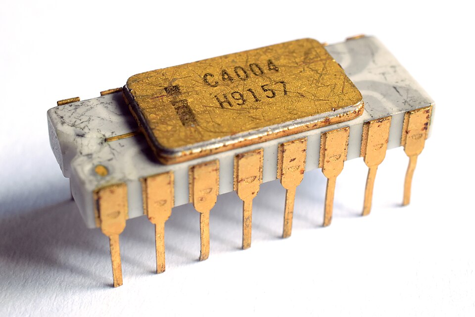
Bell Labs, 1947First transistor
First microchip
TSMC, 1987
~2 nm (TSMC)领尖节点(2025年)
~$630B (2024)Global chip sales
1956, Physics诺贝尔晶体管
半导体工程师设计,建造或制造从汽车刹车到核武器导弹制导系统等几乎运行地球上每一个有动力物体的集成电路. 作品大致分为两个阵营:设计工程师在软件中铺设电路并交出一个完成的蓝图,以及操作物理工厂的工序或设备工程师,称为fabs,这些蓝图一次将一些原子塞入硅.
该专业比这个站点上的大多数都年轻——第一个工作晶体管在1947年被展示出来——但是它已经成为了最后果之一. 少数集中在少数地方的公司现在控制着制造最先进芯片所需的机器和诀窍,每个与人工智能、国防或经济增长有利害关系的政府都决定了这一点。
这种集中使这项工作异常高涨。 一家荷兰公司建造了先进的印刷机;一家台湾公司制造了世界上大多数最先进的逻辑芯片;在华盛顿书写了出口管制规则,各国工程师可以合法地向它们出售设备或专门知识。 几乎没有什么工程事业 如此接近于大国政治。
深入这份职业
半导体工程师设计或制造几乎所有现代设备里的晶体管:晶圆给出裁决,良率说话,地缘政治则决定你能站在哪条产线上。对在中国大陆从业者而言,监管口径、客户预期、交付节奏与团队协作必须进入判断,不能只复制海外岗位描述的光鲜部分。
设计、工艺与晶圆的裁决
前端写RTL与版图,后端在光刻刻蚀与薄膜中把图纸变成器件。两端用PDK、设计规则与测试向量对话。晶圆电性与良率是最终法官。中国晶圆厂与设计公司扩张中,设备材料与EDA约束让可制造性成为比论文更硬的指标。对在中国大陆从业者而言,监管口径、客户预期、交付节奏与团队协作必须进入判断,不能只复制海外岗位描述的光鲜部分。香港与台湾的资质路径、舆论与合规细节可能不同,跨区域发展前应单独核对,不要假设华语地区都一样。真正拉开差距的,往往是压力下能否把复杂权衡讲清并留下可复查依据,而不是只会完成表面上的标准动作。把这类判断写进可复查的记录,比事后用情怀解释疏漏更负责任。
洁净室、批次与良率
洁净纪律、批次追溯与SPC是工艺日常。一次污染可毁掉整批。设计侧被时序、功耗与可测性驱赶。机台稼动率把工厂变成24小时系统,996常以排班出现,安全与疲劳管理是缺陷与工伤的前因。对在中国大陆从业者而言,监管口径、客户预期、交付节奏与团队协作必须进入判断,不能只复制海外岗位描述的光鲜部分。香港与台湾的资质路径、舆论与合规细节可能不同,跨区域发展前应单独核对,不要假设华语地区都一样。真正拉开差距的,往往是压力下能否把复杂权衡讲清并留下可复查依据,而不是只会完成表面上的标准动作。把这类判断写进可复查的记录,比事后用情怀解释疏漏更负责任。把这类判断写进可复查的记录,比事后用情怀解释疏漏更负责任。
学校、筛选与地缘门槛
微电子物理与电气工程是常见背景,笔试与洁净室实习是过滤器。出口管制与实体清单让国际流动变复杂。先进封装、化合物半导体与汽车芯片开辟旁路,基础仍是器件物理与统计学直觉。对在中国大陆从业者而言,监管口径、客户预期、交付节奏与团队协作必须进入判断,不能只复制海外岗位描述的光鲜部分。香港与台湾的资质路径、舆论与合规细节可能不同,跨区域发展前应单独核对,不要假设华语地区都一样。真正拉开差距的,往往是压力下能否把复杂权衡讲清并留下可复查依据,而不是只会完成表面上的标准动作。把这类判断写进可复查的记录,比事后用情怀解释疏漏更负责任。把这类判断写进可复查的记录,比事后用情怀解释疏漏更负责任。
AI布图与战略地理
机器学习辅助OPC与布局布线,加速迭代却不取消物理极限。国家战略把芯片写成安全议题,人才争夺与保密同步上升。为国造芯使命可贵,也被用来合理化过劳与忽视职业病防护。可持续团队把良率责任与休息制度一起设计。对在中国大陆从业者而言,监管口径、客户预期、交付节奏与团队协作必须进入判断,不能只复制海外岗位描述的光鲜部分。香港与台湾的资质路径、舆论与合规细节可能不同,跨区域发展前应单独核对,不要假设华语地区都一样。真正拉开差距的,往往是压力下能否把复杂权衡讲清并留下可复查依据,而不是只会完成表面上的标准动作。把这类判断写进可复查的记录,比事后用情怀解释疏漏更负责任。
工作如何分岔
同一头衔下常见的五条路径——专长、场景与生涯形态。
芯片设计公司
数字设计/RTL工程师
把功能写成可综合逻辑,并关闭验证漏洞。
后端设计
物理设计工程师
在工艺约束下完成布局布线与时序收敛。
晶圆厂
工艺/良率工程师
用数据把缺陷与工艺窗口逼到可量产。
先进工艺研发
器件/集成工程师
在新结构与材料上证明可重复性能。
验证团队
验证/可测性工程师
设计测试覆盖,让缺陷在出货前被抓住。
各国读法不同
同样的行当,门槛、地位与日常不同。按各语言读者真正搜索的语境重写。
美国 — 半导体工程师的市场与门槛
在美国,半导体工程师的机会、薪酬与准入规则因州、行业和雇主类型差异很大。大型机构提供结构化训练与执照路径,初创与自由职业更灵活也更不稳定。对接中美业务时,英语沟通、签证与合规意识通常和专业技能同等重要。
韩国 — 大企业节奏与本地语境
韩国的半导体工程师岗位常见于大企业、成长型公司与专业服务网络,工作节奏快且层级协作明显。韩语与本地习惯影响表现;协作时需预留文化与合规差异,勿把加班文化直接当成行业标准。
日本 — 流程、细节与长期关系
日本市场里,半导体工程师常强调流程完整、质量细节与长期信任。资格、年功或轮岗影响晋升;外企与本土机构对英语和速度的期待不同,选雇主几乎等于选工作方式。把这类判断写进可复查的记录,比事后用情怀解释疏漏更负责任。
德国 — 规范、培训与技术深度
德国的半导体工程师受职业教育、行业标准与劳动制度塑造,文档与长期责任很重。专精路线清晰;适应正式流程与工时边界是门槛,也是理解欧洲合规与工会话语的起点。把这类判断写进可复查的记录,比事后用情怀解释疏漏更负责任。
英国 — 资格路径与伦敦集聚
英国的半导体工程师机会常向伦敦及专业网络集中,资格、雇主品牌与合同制影响进入路径。生活成本与稳定性需一并衡量;脱欧后监管细节仍影响跨境业务与证书互认。把这类判断写进可复查的记录,比事后用情怀解释疏漏更负责任。
新加坡 — 区域枢纽与华语市场连接
新加坡常把半导体工程师连到东南亚客户、跨国总部与华语商业网络。英语是协作语言,但大陆、香港、台湾的监管与数据语境不能等同;跨时区与多元合规是日常。把这类判断写进可复查的记录,比事后用情怀解释疏漏更负责任。
档案图集
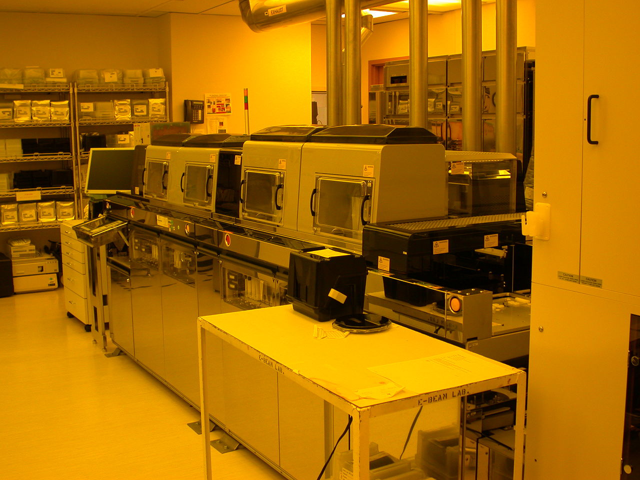
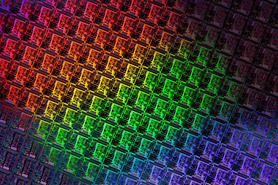
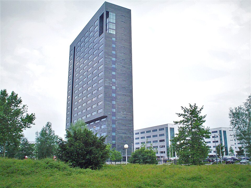
为本职业自托管的 Commons CC/PD 图片。
为什么态度在这份工作里很重要
半导体工程师的器件与工具链知识必要;但态度决定良率异常是被深挖还是下批再看,以及洁净纪律是否在疲倦时仍成立。国内常见的是用使命感、情怀或“关键节点”把无偿加班说成觉悟,拒绝者被贴上不够热爱的标签。
晶圆不接受口头保证
汇报里的基本收敛改变不了缺陷密度。态度决定你是否把SPC告警当真实事件。掩盖异常批次可能保住当月奖金,毁掉客户信任与制程窗口。国内常见的是用使命感、情怀或“关键节点”把无偿加班说成觉悟,拒绝者被贴上不够热爱的标签。996与大小周并不自动等于专业深度;过劳会制造你本想防止的疏漏,清醒才是安全裕度。可持续的团队把训练、交接与休息写进编制,而不是靠年轻人的热情无限填坑。把这类判断写进可复查的记录,比事后用情怀解释疏漏更负责任。把这类判断写进可复查的记录,比事后用情怀解释疏漏更负责任。把这类判断写进可复查的记录,比事后用情怀解释疏漏更负责任。把这类判断写进可复查的记录,比事后用情怀解释疏漏更负责任。
洁净室纪律是集体产品
一个人的抄近路污染整批。对规程的态度比个人聪明更影响良率。班次文化要么互相提醒,要么互相掩护违规。国内常见的是用使命感、情怀或“关键节点”把无偿加班说成觉悟,拒绝者被贴上不够热爱的标签。996与大小周并不自动等于专业深度;过劳会制造你本想防止的疏漏,清醒才是安全裕度。可持续的团队把训练、交接与休息写进编制,而不是靠年轻人的热情无限填坑。把这类判断写进可复查的记录,比事后用情怀解释疏漏更负责任。把这类判断写进可复查的记录,比事后用情怀解释疏漏更负责任。把这类判断写进可复查的记录,比事后用情怀解释疏漏更负责任。把这类判断写进可复查的记录,比事后用情怀解释疏漏更负责任。
地缘压力放大过劳叙事
卡脖子话语让拒绝加班变成觉悟问题。战略重要不等于科学上需要连续失误。态度包括区分真正紧急与表演性紧急。国内常见的是用使命感、情怀或“关键节点”把无偿加班说成觉悟,拒绝者被贴上不够热爱的标签。996与大小周并不自动等于专业深度;过劳会制造你本想防止的疏漏,清醒才是安全裕度。可持续的团队把训练、交接与休息写进编制,而不是靠年轻人的热情无限填坑。把这类判断写进可复查的记录,比事后用情怀解释疏漏更负责任。把这类判断写进可复查的记录,比事后用情怀解释疏漏更负责任。把这类判断写进可复查的记录,比事后用情怀解释疏漏更负责任。把这类判断写进可复查的记录,比事后用情怀解释疏漏更负责任。
压力之下仍立得住的态度
不是口号,而是这份工作真正看重的五种具体姿态。
把良率告警当事件
触发调查与隔离,不等下一批看看再说。统计过程控制的意义在于及时,不在装饰看板。国内常见的是用使命感、情怀或“关键节点”把无偿加班说成觉悟,拒绝者被贴上不够热爱的标签。996与大小周并不自动等于专业深度;过劳会制造你本想防止的疏漏,清醒才是安全裕度。可持续的团队把训练、交接与休息写进编制,而不是靠年轻人的热情无限填坑。把这类判断写进可复查的记录,比事后用情怀解释疏漏更负责任。把这类判断写进可复查的记录,比事后用情怀解释疏漏更负责任。
疲倦时仍守洁净规程
不因赶工省略更衣与物料纪律。污染成本以整批计,远高于多花的三分钟。国内常见的是用使命感、情怀或“关键节点”把无偿加班说成觉悟,拒绝者被贴上不够热爱的标签。996与大小周并不自动等于专业深度;过劳会制造你本想防止的疏漏,清醒才是安全裕度。可持续的团队把训练、交接与休息写进编制,而不是靠年轻人的热情无限填坑。把这类判断写进可复查的记录,比事后用情怀解释疏漏更负责任。把这类判断写进可复查的记录,比事后用情怀解释疏漏更负责任。
设计为可制造
追求性能时同步考虑工艺窗口与可测性,不把问题丢给晶圆厂。跨团队尊重是良率隐藏参数。国内常见的是用使命感、情怀或“关键节点”把无偿加班说成觉悟,拒绝者被贴上不够热爱的标签。996与大小周并不自动等于专业深度;过劳会制造你本想防止的疏漏,清醒才是安全裕度。可持续的团队把训练、交接与休息写进编制,而不是靠年轻人的热情无限填坑。把这类判断写进可复查的记录,比事后用情怀解释疏漏更负责任。把这类判断写进可复查的记录,比事后用情怀解释疏漏更负责任。
文档对下一批诚实
把已知风险与临时对策写进转移单,不靠口头部落知识。人员流动快时,纸面是唯一记忆。国内常见的是用使命感、情怀或“关键节点”把无偿加班说成觉悟,拒绝者被贴上不够热爱的标签。996与大小周并不自动等于专业深度;过劳会制造你本想防止的疏漏,清醒才是安全裕度。可持续的团队把训练、交接与休息写进编制,而不是靠年轻人的热情无限填坑。把这类判断写进可复查的记录,比事后用情怀解释疏漏更负责任。把这类判断写进可复查的记录,比事后用情怀解释疏漏更负责任。
区分战略加班与无效加班
在真正机台窗口全力以赴,拒绝用通宵掩盖计划无能。态度是对物理与同事睡眠的双重诚实。国内常见的是用使命感、情怀或“关键节点”把无偿加班说成觉悟,拒绝者被贴上不够热爱的标签。996与大小周并不自动等于专业深度;过劳会制造你本想防止的疏漏,清醒才是安全裕度。可持续的团队把训练、交接与休息写进编制,而不是靠年轻人的热情无限填坑。把这类判断写进可复查的记录,比事后用情怀解释疏漏更负责任。把这类判断写进可复查的记录,比事后用情怀解释疏漏更负责任。
分辨真假的时刻
把简历用语和实际执行区分开来的具体情境。
出货前的良率下跌你是否坚持分析根因,还是为交期放行可疑批次?态度决定短期交付与长期客户哪一个优先。国内常见的是用使命感、情怀或“关键节点”把无偿加班说成觉悟,拒绝者被贴上不够热爱的标签。996与大小周并不自动等于专业深度;过劳会制造你本想防止的疏漏,清醒才是安全裕度。可持续的团队把训练、交接与休息写进编制,而不是靠年轻人的热情无限填坑。把这类判断写进可复查的记录,比事后用情怀解释疏漏更负责任。把这类判断写进可复查的记录,比事后用情怀解释疏漏更负责任。
夜班有人简化更衣你是否提醒并上报,还是当没看见?集体沉默是污染的共谋。国内常见的是用使命感、情怀或“关键节点”把无偿加班说成觉悟,拒绝者被贴上不够热爱的标签。996与大小周并不自动等于专业深度;过劳会制造你本想防止的疏漏,清醒才是安全裕度。可持续的团队把训练、交接与休息写进编制,而不是靠年轻人的热情无限填坑。把这类判断写进可复查的记录,比事后用情怀解释疏漏更负责任。把这类判断写进可复查的记录,比事后用情怀解释疏漏更负责任。
设计规则临界的创新你是否要求额外验证,还是被进度说服?临界设计常在量产时爆炸。国内常见的是用使命感、情怀或“关键节点”把无偿加班说成觉悟,拒绝者被贴上不够热爱的标签。996与大小周并不自动等于专业深度;过劳会制造你本想防止的疏漏,清醒才是安全裕度。可持续的团队把训练、交接与休息写进编制,而不是靠年轻人的热情无限填坑。把这类判断写进可复查的记录,比事后用情怀解释疏漏更负责任。把这类判断写进可复查的记录,比事后用情怀解释疏漏更负责任。
用使命感要求连续第三周通宵你是否要求重新排计划与人力,还是把身体当耗材?芯片需要清醒的人,不是耗尽的符号。国内常见的是用使命感、情怀或“关键节点”把无偿加班说成觉悟,拒绝者被贴上不够热爱的标签。996与大小周并不自动等于专业深度;过劳会制造你本想防止的疏漏,清醒才是安全裕度。可持续的团队把训练、交接与休息写进编制,而不是靠年轻人的热情无限填坑。把这类判断写进可复查的记录,比事后用情怀解释疏漏更负责任。把这类判断写进可复查的记录,比事后用情怀解释疏漏更负责任。
"使命感"变成伤害的地方
国产替代话术下的过劳
半导体被写成民族事业时,996更容易被道德化。年轻人加班被夸成扛起产业链,拒绝被说不懂大局。真正产业升级需要可持续工程文化、职业病防护与可预期休假;否则人才用脚投票,良率用缺陷投票。使命感是方向盘,不是油门踩死的理由。国内常见的是用使命感、情怀或“关键节点”把无偿加班说成觉悟,拒绝者被贴上不够热爱的标签。996与大小周并不自动等于专业深度;过劳会制造你本想防止的疏漏,清醒才是安全裕度。可持续的团队把训练、交接与休息写进编制,而不是靠年轻人的热情无限填坑。把这类判断写进可复查的记录,比事后用情怀解释疏漏更负责任。把这类判断写进可复查的记录,比事后用情怀解释疏漏更负责任。
职业画像
- 抗AI60
- 薪酬82
- 入行门槛78
- 自主性55
- 需求90
- 影响力96
对AI有多暴露?
Moderate
具体,定义明确的任务——从图像中分解华费缺陷,优化芯片的物理布局,生成第一稿验证测试——已经相当快,可以让AI工具处理. 很难实现自动化的是,在物理上调整一个法布工具,它的行为与下一线的双胞胎略有不同,诊断出一个没有先例的缺陷,当决定影响到一批价值数百万美元的瓦佛时,要承担责任。
AI与未来 →
理解这一职业的七个角度
01
起源与演变
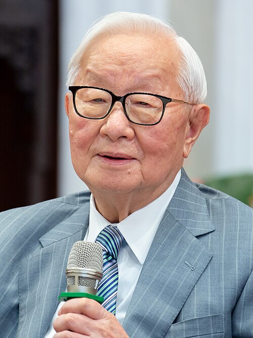
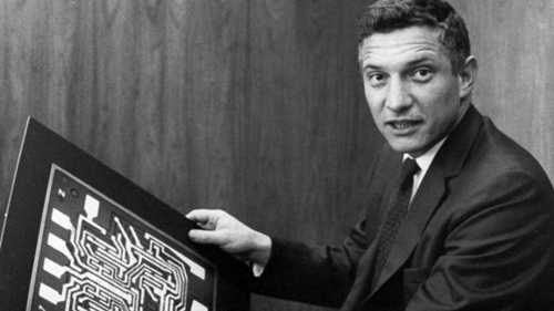
从贝尔实验室的第一台晶体管通过Kilby,Noyce,摩尔定律,Morris Chang的铸币模型,EUV Lithography和今天的芯片地缘政治.
阅读 →
02
文化与地位
从1950年代的'boffin'蒙昧到奇普战争畅销书——半导体工程师的公众形象如何随着业界的利害关系而转变.
阅读 →
03
大学与入行路径
真正的学位,真正的fab-croup学校 从台湾到荷兰, 和资格门 决定谁设计或制造芯片。
阅读 →
04
实务与诀窍
真正的能力, 一天的芯片外壳, 贸易的仪器, 和产量-工程技术 经验丰富的工程师。
阅读 →
05
传奇人物
从贝尔实验室的晶体管发明者到莫里斯·张的铸造模型和索菲·威尔逊的ARM芯片——塑造芯片制作方式的人.
阅读 →
06
AI与未来
具体,诚实的看看哪些芯片设计和fab任务AI已经自动化了,它抵制自动化,以及工作是如何变化的.
阅读 →
07
薪酬与市场
来自美国、台湾、韩国、荷兰、德国和中国的实际工资带,加上需求趋势和雇用最多工程师的雇主。
阅读 →
常见问题
一个半导体工程师整天做什么?
这在很大程度上取决于专业。 一个芯片设计工程师在软件上度过了一天,铺设了电路,并模拟了它们在制造任何东西之前的行为. 工序或设备工程师的工作更靠近实际的法布地板,对沉积、牵引和图案硅瓦的机器进行调制,并追查一批产量下降的原因。
在半导体工作需要研究生学位吗?
一个学士在电气工程,材料科学或物理学方面足以成为许多入门级设计和法布角色. 研究重的姿势——高级过程开发,新颖设备架构,在国家实验室工作——通常期望有硕士或博士学位,因为所涉及的物理在大约10纳米以下会真正困难.
来自AI的半导体工程有风险吗?
一些任务已经是: AI工具现在帮助放置和路由芯片布局,对wafer图像中的缺陷进行分类,并生成第一稿验证测试. 在物理上调整一个价值数百万元的蚀刻工具,诊断出以前从未见过的缺陷,或者当一整批瓦片被刮掉时,要承担责任,仍然很难交给模型。
半导体工程师能挣多少钱?
它因国家和专长而大不相同。 在美国,该领域的工程师通常收入很高,有六个数字,随着资历的提高而急剧上升。 在台湾,大多数先进芯片实际上都是制作的,因此与该行业的全球重要性相比,基础工资名列前茅,尽管在全球人才短缺的情况下,基础工资一直在快速上升。
法布和无边公司有什么区别?
A fab是一家生产芯片的物理工厂;拥有和运行一个每代技术花费数百亿美元. 像Nvidia或Qualcomm这样的无名公司,设计芯片但支付TSMC或三星等铸币厂制造这些芯片的费用——由莫里斯·张铸币厂的铸币模型所普及的分拆,始于1987年.
为什么台湾对芯片制造如此重要?.
TSMC成立于1987年的Hsinchu,建造了数十年的制造专有技术,竞争者一直努力复制,现在编造了世界上绝大多数最先进的逻辑芯片. 这种集中,有时被称为台湾的"硅盾",是该岛被远在东亚以外的政府视为战略批评的中心原因.
摩尔的律法是什么,还是真的吗?
戈登·摩尔(Gordon Moore)在1965年观察到,芯片上的组件数量每年大约翻一番,后来改为每两年一次. 然后,该行业花了60年时间将这一预测作为打击而不是发现物理学的路线图。 自2010年代中期以来,扩展速度急剧放缓,大多数工程师现在将其描述为不仅仅是法律的经济目标。
半导体工程师能远程工作吗?
很少,对于大部分的球场。 工艺和法布工程师必须实际出现在清洁室地板上,以运行工具,检查瓦片并应对设备警报. 芯片设计工程师有更大的灵活性,因为很多工作发生在软件中,但即使是设计团队也常常需要现场访问安全服务器和出口控制工具.
嵌入此榜单
将这段代码粘贴到您的博客或网站,榜单会保持最新。
已复制